
Page 74 - TSMC 2018 Annual Report
P. 74
5 2 Technology Leadership
5 2 1 R&D Organization and Investment
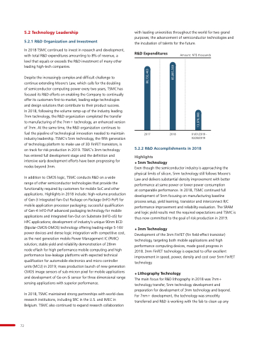
In 2018 TSMC continued to invest in in in research and development with total R&D expenditures amounting to to 8% of revenue a a a level that equals or exceeds the the R&D investment of many other leading high-tech companies Despite the increasingly complex and difficult challenge to continue extending Moore’s Law which calls for the doubling
of semiconductor computing power every two years TSMC has focused its R&D efforts on on enabling the Company to continually offer its customers first-to-market leading-edge technologies and design solutions that contribute to their product success In 2018 following the the volume ramp-up of the the industry leading 7nm technology the the R&D organization completed the the transfer to manufacturing of the 7nm+ technology an an an enhanced version of 7nm At the the same time the the R&D organization continues to fuel the pipeline of technological innovation needed to maintain industry leadership TSMC’s 5nm technology the fifth generation of of technology platform to to make use of of 3D FinFET transistors is is on on track for risk production in 2019 TSMC’s 3nm technology has entered full development stage and and the definition and and intensive early development efforts have been progressing for for nodes beyond 3nm In addition to CMOS logic TSMC conducts R&D on on on a a wide
range of other semiconductor technologies that provide the the functionality required by customers for mobile SoC and other applications Highlights in in 2018 include: high-volume production of Gen-3 Integrated Fan-Out Package Package on Package Package (InFO-PoP) for mobile application processor packaging successful qualification of Gen-4 InFO-PoP advanced packaging technology for mobile applications and Integrated Fan-Out on on Substrate (InFO-oS) for HPC applications development of industry’s unique 90nm BCD (Bipolar-CMOS-DMOS) technology offering leading-edge 5-16V power devices and dense logic integration with competitive cost as the next generation mobile Power Management IC IC (PMIC) solution stable yield and reliability demonstration of 28nm
node eFlash for for high high performance mobile computing and high high performance low-leakage platforms with expected technical qualification for automobile electronics and micro controller units (MCU) in 2019 mass production launch of new generation CMOS image sensors of sub-micron pixel for mobile applications and development of Ge-on-Si sensor for three dimensional range sensing applications with superior performance In 2018 TSMC maintained strong partnerships with world-class research institutions including SRC in in in in in the U S S and IMEC in in in in in Belgium TSMC also continued to expand research collaboration
with leading universities throughout the world for two grand purposes the advancement of semiconductor technologies and the the incubation of talents for the the future R&D Expenditures
Amount: NT$ thousands
72
2017 2018 01/01/2019 - 02/28/2019
5 2 2 2 2 2 2 R&D Accomplishments in 2018 Highlights • 5 n n n m m T e e e e c h h h h h h n n n o o o l l o o o g g g g y Even though the the semiconductor industry is approaching the the physical limits of silicon 5nm technology still follows Moore’s Law and delivers substantial density improvement with better performance at same power power or or lower power power consumption
at comparable performance In 2018 TSMC continued full development of 5nm focusing on manufacturing baseline process setup yield learning transistor and interconnect R/C performance improvement and reliability evaluation The SRAM and and logic yield results met the required expectations and and TSMC is thus now committed to the goal of risk production in 2019 • 3 3 n n n m m T e e e e e c h h n n n o o o o l l o o o o g y Development of the 3nm FinFET (Fin field-effect transistor) technology targeting both mobile applications and high performance computing devices made good progress in in 2018 3nm FinFET technology is expected to offer excellent improvement in in speed power density and cost over 5nm FinFET technology • L i i i t t h h h h h o o o o o o g g g r r a a p
h h h h h y y T T e e c c h h h h h n n o o o o o o l l o o o o o o g g g y y The main focus for R&D lithography in in 2018 was 7nm+ technology technology transfer 5nm technology technology development and preparation for development of 3nm technology and beyond For 7nm+ development the technology was smoothly transferred and R&D is working with the fab to clean up any 13 078 088
80 732 463
85 895 569
