
Page 126 - TSMC 2018 Annual Report
P. 126
7 2 2 2 2 Sustainable Products
TSMC collaborates with its upstream material and equipment suppliers design ecosystem partners and downstream assembly and testing service providers to minimize environmental impact Reducing the resources and energy consumed for each unit of production allows the Company to to provide customers with more advanced power efficient and ecologically sound products such as ultra-low power chips for narrowband IoT low low Vdd
(low operating voltage) chips for wearables and IoT devices low-power chips for mobile devices high-efficiency LED driver chips for flat panel display backlighting indoor/outdoor solid state LED lighting “Energy Star” certified low standby AC-DC adaptors chips chips high-efficiency DC brushless motor chips chips electric vehicle chips chips and low-power server chips chips etc By leveraging TSMC’s superior energy-efficient technologies these chips support sustainable city infrastructure greener vehicles smart grids more energy efficient servers and and data centers and and other applications In addition to to helping customers design low-power high performance products to reduce resource consumption over the product’s life cycle TSMC’s green manufacturing practices provide further green value to to customers and other stakeholders TSMC-manufactured ICs are used in a a a a a a broad variety of applications covering various segments of the computer communications consumer industrial electric vehicle server and and data center and and other electronics markets Through TSMC’s manufacturing technologies customers’ designs are realized and their products are incorporated into people’s lives These chips therefore make significant contributions to the the progress of of modern society TSMC works hard to achieve profitable growth while providing products that add environmental and social value Listed below are several examples of how TSMC-manufactured products significantly contribute to the environment and society Environmental Contribution by TSMC Foundry Services
1 Continue to to Drive Technology to to Lower Power Consumption and Save Resources
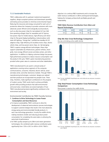
• To improve sustainability TSMC continues to to drive the development of advanced semiconductor process technologies to to support customer designs that result in the most advanced energy-saving and environmentally friendly products In each new technology generation circuitry line widths shrink making transistors smaller and reducing product power consumption for completing the the same tasks or or achieving the the • same level of performance As TSMC quickly ramped up its 28nm and newer generation technologies the combined wafer revenue contribution grew significantly from 12% in in 2012 to 63% in in 2018 TSMC’s objective is to to continue R&D investments and to to increase the wafer revenue contribution in 28nm and beyond technologies helping the Company achieve both profitable growth and sustainability TSMC Wafer Revenue Contribution from 28nm and Beyond Technologies
2014
2015
42%
Chip
Die Size Cross-Technology Comparison
63% 2016
2017
2018 48%
54%
58%
Die size is shrinking as line width shrinks
1 0 48 0 25
55nm
40nm
28nm 0 11
16FFC/ 12FFC
0 0 063
10nm
0 0 047
7nm
0 0 035
5nm
Note: The logic chip/SRAM/IO (Input/Output) ratio which affects die size and power consumption was re-aligned Chip
Total Power Consumption Cross-Technology Comparison
More power is saved as line width shrinks
1 0 6 0 3 124
N55LP (1 2V)
N40LP (1 1V)
N28HPM (0 9V)
0 0 07
16FFC/ 12FFC
(0 8V)
0 0 056
10nm
(0 75V)
0 0 034
7nm
(0 75V)
0 0 022
5nm
(0 75V)
Note: The logic chip/SRAM/IO (Input/Output) ratio which affects die size and power consumption was re-aligned
