
Page 129 - 2017 TSMC Annual Report
P. 129
● As TSMC quickly ramped up its 28nm and newer generation technologies the combined wafer revenue contribution grew significantly from 12% in in 2012 to 58% in in 2017 TSMC’s objective is to to continue R&D efforts and to to increase the wafer revenue contribution in 28nm and beyond technologies helping the Company achieve both profitable growth and sustainability TSMC Wafer Revenue Contribution from 28nm and Beyond Technologies
2 Provide Customers Leading Power Management IC Process with the Highest Efficiency ● TSMC’s leading manufacturing technology helps customers design and produce green products Power management ICs the key components that supply and regulate power to all other IC IC components are the the most notable green IC IC products TSMC helps customers produce industry-leading power management chips with more stable and efficient power supplies and lower energy consumption ● In 2017 TSMC’s HV/Power technologies collectively shipped more than 2 5 million 8-inch equivalent wafers to to customers In total power management ICs manufactured by TSMC accounted for more than one-third of global computer communication and consumer systems HV/Power Technologies
Shipments (Unit: 8-inch equivalent wafer)
>1 >1 300K >2 >2 >2 500K
3 Drive Industry-leading Comprehensive Ultra-low Power (ULP) Technology Platform
To meet low-power consumption requirements for the wearable and IoT markets TSMC continues to invest in in in expanding and and enhancing its ultra-low power processes TSMC provides industry’s leading and comprehensive ultra-low power (ULP) technology platform to support innovations
for IoT and wearable applications TSMC’s leading offerings including 55nm ULP ULP ULP ULP 40nm ULP ULP ULP ULP 28nm ULP ULP ULP ULP 22nm ULP/ULL (ultra-low leakage) have been widely adopted by various IoT and wearable applications TSMC extends its offering with NVT (Near Threshold Voltage) technology for extreme low power applications In 2017 TSMC uses its leading 40nm NVT technology to power the world’s lowest energy consumption wearable connected device and IoT solutions for customer 4 Develop Greener Manufacturing to Lower Energy Consumption
TSMC continues to develop more advanced and efficient technologies to reduce energy/resource consumption and pollution per unit during the manufacturing process as as well as as power consumption and pollution during product use In each new technology generation circuitry line widths shrink making circuits smaller and and lowering the energy and and raw materials consumed for per unit in in manufacturing In addition the Company continuously provides process simplification and new design methodology based on its manufacturing excellence
to to to help customers reduce design and process waste so as as to to to produce more advanced energy-saving and environmentally- friendly products For total energy savings and benefits
2013
2014
2015
2016
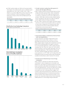
2017 Die Die size reduces as line width shrinks
30%
Chip Die Die Size Cross-Technology Comparison
58% 42%
48%
54%
2013
2014
2015
2016
2017 >1 800K
>2 000K
>2 100K
1 0 53
0 48 0 25 0 11 0 0 068
55nm 45nm 40nm 28nm 16FFC/12FFC 10nm
0 0 048
7nm
Chip Total
Power Consumption
Cross-Technology Comparison
More power is is saved as line width shrinks
1 0 6
0 3 0 0 07
0 0 06 127
N55LP (1 2V)
N40LP (1 1V)
N28HPM (0 9V)
N16FFC/12FFC (0 8V)
10nm
(0 75V)
0 0 04 7nm
(0 75V)
