R&D Achievements
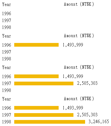
TSMC has the largest and the most outstanding semiconductor R&D organization in Taiwan and in the world's dedicated foundry industry. Over the last three years, TSMC's overall R&D investment has increased even more rapidly than revenue growth, reflecting our determination to provide customers with world-class, leading-edge technology. In 1998 alone, TSMC spent over NT$3.2 billion on R&D. Also in 1998, TSMC won the highest possible honor among the awards for Industrial Technology Advancement presented by the Ministry of Economic Affairs in Taiwan.
In 1998, TSMC obtained 220 US patents and 170 ROC patents, ranking ninth in the world for the acquisition of US patents for IC process technology, and acquiring more patents than any other Taiwan company. This achievement led Taiwan's National Bureau of Standards to award TSMC the Gold Medal Prize at the National Invention Awards.
TSMC R&D leads the IC foundry industry and now matches worldwide IC industry leaders in the development and introduction of low voltage, low power and high performance logic process technology. After the successful transfer and ramp up to mass production of the high performance 0.25µm logic process, in 1998 TSMC R&D developed and introduced the next advancement, 0.18µm logic technology. TSMC's 0.18µm logic process has the most aggressive design rules in the world, as well as very advanced low voltage, high performance transistors with gate length of less than 0.15µm. This new process technology is capable of supporting microprocessors and graphics chips that operate at speed in excess of 600MHz. TSMC's 0.18µm technology also has the most advanced low-k (low dielectric constant) insulator integrated with conventional AlCu (aluminum-copper) metallization to reduce interconnect RC (resistance/ capacitance) delay and dramatically enhance the performance of our customers' products. In addition, TSMC has demonstrated the most advanced copper interconnect process as a fully design-rule-compatible option to our 0.18µm logic technology. TSMC's copper interconnect process has the world's tightest design rules in this generation and is the first from a dedicated foundry.
TSMC has the foundry industry's largest in-house mask fabrication facility. We provide excellent quality and cycle time to support fast prototyping and production. In 1998, our mask technology R&D and in-house mask shop demonstrated advanced optical-proximity-correction (OPC) mask technology as well as phase-shift mask (PSM) technology. Both these techniques are used in our 0.25µm and 0.18µm logic processes and will be the key to developing future generation technologies.
TSMC R&D did pioneering work on embedded memory for rapidly developing system-on-a-chip (SOC) applications. In 1998, we enriched our SOC technology menu with the release of a very dense high-speed embedded SRAM for 0.25µm and 0.18µm generation logic technologies in microprocessor and graphics applications. We also released 0.35µm embedded DRAM for disk drives and multi-media applications, as well as 0.35µm embedded Flash memory for micro-controllers and wireless applications. These embedded memory processes are supported by a complete set of compilers, design kits, and test support to facilitate customer design procedures and to speed the introduction of SOC products.
In the area of stand-alone memory, TSMC R&D introduced the world's smallest 0.25µm 4T SRAM process last year. An extremely low-standby 4Mb 6T SRAM process was also released for applications that demand low-power. We are currently developing and prototyping future generations of embedded and stand-alone memory processes. Some examples are: 0.15µm and 0.13µm embedded SRAM; 0.18µm high-speed low-power SRAM; 0.25µm and 0.18µm embedded DRAM; 0.25µm and 0.18µm embedded Flash memory, and 0.22µm EEPLD memory processes.
In 1998, TSMC R&D introduced a 0.25µm mixed-signal process with a rich set of modular analog devices and passive components, for example, high-Q metal-insulators-metal capacitors, precision resistors and low threshold devices. They are used in modems, audio, and other mixed-digital-analog SOC, as well as wireless baseband applications. The process will soon be enriched with modular high-Q inductors for RF and wireless applications. Development of advanced next-generation 0.18µm mixed-signal, baseband, and RF technologies is underway to provide a complete set of SOC solutions.